I've had significant issues with the new Ubuntu GUI and Gnome 3.0; ranging from irritations (difficulty to create launchers) to bugs (mouse stops responding). If you are googling around I'm sure you've seen the near universal cry of dismay. If there is one message to send Canonical (if any of you ever read this posting) it would be that while its a great idea to "dumb down" the interface so a single GUI will work between your desktop and touch machines, you can't disable the advantages available through a mouse interface!
Anyway, here is what I did to make it workable. These are mostly culled from various web sources; they are not my original work.
The Arduino is great; a microController you can actually do something with for 30 bucks! Ok, but your train layout needs 5 of them ($150), your home sensor network needs 10 + $40 xbee cards (clocking in at $700!). Or the mere fact that your want to KEEP your projects around means that you get nailed for 30 bucks over and over again.
But wait a second... the AVR328p is a 3 dollar chip! And the AVR ATMega48 (pin compatible but with a LOT less space) is 2 bucks (for 10)! And if your requirements are extremely minimal, there's the ATTINY13 which comes in as little as 60 cents -- but in an inconvenient package (you'll be better off spending another 4 dimes and getting one for 1 buck).
Let's hack up a bunch of these chips so next project we'll have lots of choices...
In the last posting I described how I made a few PCBs to act as SMT breakouts. I've discovered that this seems to be a pretty ideal job for DIY PCB work! To mount thru-hole stuff, you need the hole -- and that means hand drilling... but a small breakout board can be done on a single side, and its possible to use .1" Right Angle headers soldered onto an oval thru-hole pad so you don't even need to drill the hole for the breakout header.
In my last posting I finished with the circuit board ironed onto the blank PCB. It turns out that the final steps are quite easy. First you get some etchant. I used ferric chloride from Radio Shack, but I wish I had used muriatic acid and hydrogen peroxide as it seems slightly better for the environment. I poured the etchant in a leftover food container (now forever dedicated to PCB etching) and left the boards in for about 30 minutes. I used a twisted wire hanger to keep my fingers out of the etchant:
Then rinse the board in lots of water, and leave the tap running to dilute any drips of etchant solution that go down your drain. When you're done, put the top on the container (make sure it seals!) and store for next time.
To remove the laser printer toner, I tried a few paint removers, liquid sanders, etc. Nothing really worked. It turns out that Acetone (nail polish remover) is required. Its available in the paint section of hardware stores, and is absolutely amazing at the job. 2 swipes with a rag daubed in Acetone cleans the toner like wiping milk off a table!
Next I soldered the parts on to the PCBs using a toaster oven. I was concerned that the lack of a solder mask might make the solder bridge across PCB pads because its impossible to keep the solder paste onto pads. In fact, I don't even bother, I just paint a thin line down across all the pads in a row (see my earlier post on DIY SMT soldering techniques here). But in fact, the solder balled up nicely as you can see here:
These are tiny SOIC-8 and SOT-23/5 parts. I left the chip off the rightmost SOT-23/5 to see how well the solder wicked onto the pads. Before putting it in the oven, the space between all the pads was completely covered with solder paste -- the wicking works great!
I cut some of these boards with a hobbiest bandsaw, like you can get for $200 at Home Depot. But its even easier to cut them by scoring the front an back with a ruler and then breaking them against the edge of table (preferably metal). Place something hard (like a metal or hardwood block) on top, grab the protruding board with pliers and then crack it by rotating the pliers downwards quickly.
One surprise was how fine a pitch may be possible. I had originally "designed" this board for professional fabrication and I accidentally left some tiny lettering on the board. Amazingly, it transferred to the PCB perfectly well! Here is a close up:
As you can see, by the ballpoint pen I put in for scale, the height of these letters is less then one millimeter! I will need to go back to the file to check, but I'll bet that the line width is just a few mils (thousandths of an inch) wide. Many professional PCB houses won't do less then 8mils! Of course, they require repeatability across hundreds of large boards -- my goal is to get a single small breakout board out of a panel with a half dozen attempts.
So basically, if the transfer works without smudging or distortion you can get amazingly fine detail. And from my limited experience it does tend to do so reliably across portions of the board that can be 2 square inches in size. This makes me believe that it may be possible to home fabricate chip-scale BGA breakout boards -- at least for small BGA packages. I have not discovered anyone who has tried it yet; so I think that will be my next experiment (as soon as I find a "fun" BGA chip)!
EDIT: Here's a photo of the SOIC8 installed on a PCB. I think that its better to put all the pins in a single row, rather then the DIP configuration because that gives you the other side of the breakout board to use to make your circuit!
Also note that no drilling is needed! Get right angle breakaway headers and then solder them to the (undrilled) thru hole pad.
EDIT 2: Here is a photo of a SOT-363 chip with a 2 mil circle indicating pin 1. To get an idea of the size, the circle is indicated by the lead of a standard 1/4 watt resistor. As you can see the 2 mil line width was etched perfectly!
Using modern components in PCB circuit board design essentially requires the use of small surface mount packages. Testing these components can be costly and time consuming if you need to have a break-out-board professionally fabricated for every component. It is possible to hand-solder extremely thin magnet wire to individual leads of a SMT package but that is a very painstaking process.
It would be much easier if individual PCBs could be hand-fabricated for the task. I dug around on the web and DIY PCB fabrication for very small parts seems quite tricky; most people use home PCBs to make larger circuits out of thru-hole parts.
However, even if multi-chip SMT designs are not feasible, it would be very valuable to be able to rapidly fabricate single chip breakout boards for SMT parts (for noobies: a breakout board is a PCB that simply brings all the pins in a SMT chip to a male header that can be plugged into a solderless breadboard). Especially small parts; if you are putting a TQFP-144 on you board there are places where you can buy breakouts. And there are fewer footprints so you could build up a "library" of breakouts. But there are tons of different packages for components ranging from 2 to 32 pins!
Making these small-pin count PCBs might be feasible (where large SMT designs are not) for several reasons. First, the PCB will be quite small, allowing you to panel multiples "tries" onto a single DIY board. You only need one success! Second, the routing will be pretty short and simple. If the pins are placed on either side of the chip the routes will be short and on a single side (so you can try the same circuit on both sides!). Finally, I think that right angle .1" headers could be used in place of straight pins, so the final board would not need to be drilled. This will save a lot of time (and painstaking work).
Here are my first attempts (ever) to use the toner transfer method to put a mask on copper PCBs. I panelized 6 SOIC-8 and 6 SOT-23/5 breakout boards onto a space about 2x3 inches:
And the back side attempts:
The basic methodology (for people who are reading this as an instructable) is to:
1. Remove all layers of your PCB except routes, pads and vias. Export it as an image (monochrome, 600 dpi). Load it up in a graphics editor (gimp), reverse the color, and horizontally mirror it.
2. Next, use a laser printer to print it onto some kind of paper. You want a paper with unique, generally undesirable properties; essentially the toner should just barely stick and it should dissolve readily in water. Four types are commonly suggested:
A) glossy paper ripped from a cheap magazine/catalog
B) glossy photo paper
C) sticker backing paper (pull the stickers off and print on the shiny side)
D) speciality PCB toner transfer paper.
3. "clean" a blank PCB with steel wool, and then iron the toner on by placing the iron at its highest setting on the paper (which is on the PCB) for about a minute. You can't move the paper relative to the PCB so some masking tape on the corners might help. Also don't push down hard, and don't move the iron around much.
4. Soak the PCB in water for about 5 minutes and then rub the paper off. You can rub quite hard; if it toner comes off then it did not transfer.
The PCB on the upper left of image 1 was made with glossy photo paper. This paper essentially did not work for me; it would glue itself to the iron and then separate from the PCB or pick it up as well. The toner was still melted at this point so most of it stayed with the paper.
The upper right image 1 board shows what happens when you push down too hard. Pressure on the melted toner caused it to spread out. So don't do that!! :-) The bottom left of image 1 was ironed on for several minutes. It got so hot it changed the copper color -- additionally the paper was extremely hard to remove. Oops! The last photo on image 1 was again done with glossy photo paper. The paper still lifted off with the iron but amazingly it left a perfect transfer in the middle! Unfortunately I doubt its repeatable.
I left board on photo 2 clean to show how the PCB should look after it has been rubbed by the steel wool. The other 3 boards on the bottom image show transfers with the sticker-backing paper with ironing times of 30seconds, 1 minute, and 1:30. I'm sure you can see which is which since they show more toner sticking. In fact, the last image has perfect transfers of 9 out of the 12 circuits! The only miss transfers are on the top of the PCB. Clearly I did not get that portion hot enough (in fact, I think that it may have been under the steam holes of the iron). Removal of the paper was pretty quick under hot water; about 5 minutes (so clearly the boards were not under the iron for too long). But the paper did not "pill" up like other web postings suggest; it mostly peeled off. After ironing, the paper it was a little browned in spots but not significantly.
Like any other craft there is clearly a bit of skill and practice required. And some experimentation is required to become familiar with your particular tools. However, so far this looks like a pretty feasible method for breakout board fabrication. In the next installment I will attempt to etch the boards and solder the parts on!
I think Eagle 6 was rushed to market :-). It resists installation on the most popular Linux distros, and when you do finally get it working it pops up with an "I'm sorry, there's a nasty bug" dialog. But Kudos to Cadsoft for admitting it!!!
Here are my notes on the installation. I think I might be missing a step or two so if you follow these and run into issues, please post a comment!!!
These instructions should also mostly work in 32 bit Linux distros, but you won't need to install as much (remove the packages with "i386", or "32" in their names).
tar xvf libpng-1.4.8*
cd libpng-*
./configure CFLAGS=-m32 --prefix=/
make check
sudo make install
32 bit distros should remove "CFLAGS=-m32" and just use this line instead:
./configure --prefix=/
[Troubleshooting] If you get the error: "configure: error: C compiler cannot create executables" check the config.log file. If the problem is: "/usr/bin/ld: cannot find crt1.o: No such file or directory" then you did not install g++-multilib gcc-multilib.
If you get: "configure: error: zlib not installed" you did not install lib32z1-dev
Bruce Perens (who did Busybox and Debian as well as defining "Open Source") has created an Open Hardware Journal (http://openhardware.org/journal/). Check out the first issue, I've got two articles in it! Ok ok, probably he needed more submissions which is why my stuff made the cut :-). But hey I'll take it!
The first article "An Open Hardware Platform for USB Firmware Updates and General USB Development" is about the USB interface on the Lightuino. I chose that topic because this interface is a cheap and tiny way to put USB in many of your projects. The interface will talk SPI to your uP or some SPI chip, or I2C (although I did not use that in the Lightuino). And it will do serial (USB CDC ACM if you need the formal acronym) or emulate an input device (USB HID). Read the article for more info, and check out my code on github here: https://github.com/gandrewstone/toastedCypressUsb
My second article "A Return To Open Devices" is about my ideas around the philosophy and driving forces behind the open hardware movement. I'm sure the people who come to open hardware do it for many different reasons; this is simply my perspective.
A few days ago I held a workshop on do-it-yourself (aka cheap) surface mount electronics techniques at a Boston artspace/hackerspace called sprout & co (http://thesprouts.org/). This was organized through the Boston Arduino meetup group. Participants got to mount a tiny QFN-24 chip (a PCA9555 io-expander) onto a QFN breakout board and then we tested them by connecting them up to an Arduino. There was one bad chip; but once that was replaced everybody's boards worked!
Here are my notes from the workshop. If you did not attend, these notes are a good tutorial on how to get started cheaply! Also, if you'd like some of the QFN breakout boards, please contact me and I will sell you a few.
Surface Mount Tools (homemade/modified):
Toaster Oven:
Got mine from the dump. Keep it simple; you don't
need to mod it with fancy temperature feedback like some web posts suggest.
Hot air “pencil”:
$30 used heat
gun (ebay) with aluminum foil to narrow and speed the air jet. Secure the aluminum foil by wrapping steel wire around the nozzle. Shape the hole in the end by forming it around a pen with your fingers. This tool is indispensable for removing and replacing chips (rework), and works great!
Cheap plastic Mechanical Pencil:
Pencil lead solder paste onto pins;
eraser dabs off too much.
PCB Vice:
You can use any clamp like this. You can probably get one for less then $10 if you look around. Just drill a hole in your desk slightly smaller then the clamp bar and stick it in upside down.
Here it is holding the boards we made, with my breadboard-to-IDE-or-RJ-45 connector in the background.
But once you do this fairly often you'll want to upgrade to a Panavise.
Soldering Iron:
You CAN use a standard cheapo wide tip soldering iron for SMT rework -- even though you can't touch just a single pin, it is sufficient to heat a single pin.
However, knockoffs of the "Hakko 936" soldering iron are pretty cheap at $50; check Amazon or ebay. And they are all you'll ever need...
Tweezers:
You use these to hand "pick-and-place" chips. Buy them from a drugstore. But don't buy the cheapest pair you can find. Buy a set that looks totally overkill for plucking nose hairs :-) -- like they were milled out of a block of metal.
Magnifying glass/bright light:
You may need these to peek at the board as it is cooking, and for rework. I'm sure you can do it on the cheap. I have a "helping hands" for the glass:
Available on ebay for 6 bucks. And the clips are actually great for other soldering jobs, like joining 2 wires. For the bright light, any portable (plug in) work light will work fine (try home depot). Once you do a lot of work you may want a "swing arm magnifying glass lamp":
Supplies:
Solder wire:
Get thin rosin core solder
Solder Paste:
Solder paste are tiny balls of solder in a flux mix that is viscous like toothpaste. It can be very expensive and require refrigeration. Don't buy that. Buy this Lodestar paste from DealExtreme. It does not require refrigeration, however, as a hobbyist you should refrigerate it so it will last you forever.
Flux:
Flux is a substance that cleans your PCB and lets the solder flow better. It is also available at DealExtreme. They often mis-name it "paste" but you'll know it is flux only because it won't be grey. Get "no-clean" or "neutral PH" (its almost all like that now).
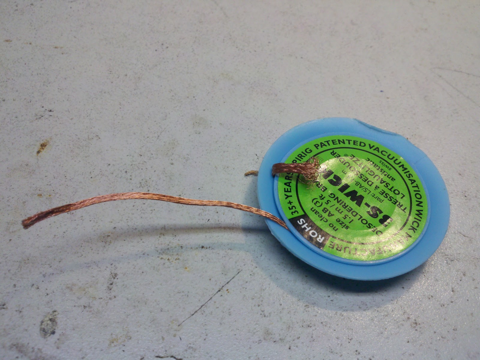
Solder Remover Braid:
This braid is necessary to remove excess solder when doing fine SMT work. Solder suckers don't work!
Step 1:
Use an oven to solder a QFN-24 part onto a
breakout board.
Mix a TINY bit of solder paste and flux to about a 60/40 mix. You don't need much. Put any extra back into the container since it contains lead so its good to generate as little hazardous waste as possible...
Too much paste and the solder will
not wick onto the pads (it will stay on the non-metal parts of the PCB or create bridges between pads -- "pads" are the metal parts of the PCB that you are trying to solder the chip's wires "pins" to)
Too much flux and the pins won't be
soldered.
Apply with your mechanical pencil (click out the lead). For
tiny QFN leads, just draw your pencil straight across all the leads. That is, cover the entire surface including between the
leads. This is important so let me emphasize: Don't try to keep the paste out of the 6mil space between the leads! That is impossible & when heated the flux will cause the paste to flow to the pads anyway.
But if there is a center square pad, use the pencil to
draw around that pad to clean any paste that would bridge the center pad to a lead (it is
very hard to fix that issue).
You need to apply a thin layer. You should be able to see the shape of the pads under the paste, but they should be obscured. But if the paste goes on clear, with just a few "dirty" spots you have too much flux in your mix.
This photo shows 6 boards with solder paste on them -- this wasn't part of the workshop, I just grabbed this photo from my archives. Perhaps the paste is on a little thick... but as you can see, no attempt was made to keep the paste away from the spaces between the pads.
Next, put the chip on with tweezers. Positioning is not critical; you can be off by a half-pin in any direction. When hot, the chip will actually float on the flux layer and surface tension will actually cause the chip to be sucked onto the pads! But if you are off by more then a half-pin, the chip might be sucked onto the wrong set of pads.
Now bake your board. You need to bake the board in a particular fashion, but its not rocket science.
Here is an example provided by Kester paste. It works fine for any paste:
Basically, you want to raise the board to 150C in a minute or two. Then wait for another minute or two so the entire board gets to that heat. This bakes out any water and lets everything expand (if you chip pops like a firecracker its ruined. You have too much water in those chips and need to bake the rest at low heat for hours to evaporate it out; its only ever happened once to me).
Next, you
bring the heat up to a max of 220-240C rapidly to melt all the solder
paste. Excessive exposure to this heat can harm the chips or melt
plastic parts so you want to keep this brief. At this point, use your
magnifying glass and a bright light to watch the paste on the board. It
will go from grey to bright shiny silver when melted (bubbling is just the flux moving around). Wait 10 more seconds after you see no more grey to make sure solder you can't see also melts. Then turn the oven off.
Now you have a choice. You can either wait with the oven door closed so the oven cools down slowly (as shown on the heat profile). Cooling slowly will mean there are fewer mechanical stresses on the board.
Or if you see any problems, you can open the oven door, pull out the tray and
reposition “tombstone” (sticking up) resistors and caps. Also if a chip is out of alignment (off by one pin for example), you can “tap”
the chip to make it position itself! When doing multiple bigger boards, you'll often find a few issues.
I'd imagine that while this cools the board faster, it is probably still less stressful then heating a portion of the board with your "air pencil". That is the only other way to reposition chips.
Debugging
Now that your board is baked and cooled, you need to visually inspect it. Look for bridges (2 pins connected) and unsoldered pins. A bridge will look more shiny then the other pins since it is a bigger solder blob. Unsoldered pins will look darker.
Unsoldered:
Apply a tiny bit of paste to solder pins. Heat the pin (and perhaps nearby pins) with an iron to melt the solder. Often you'll have added too much paste, so now check for bridges.
Bridges:
Use flux to cause the bridge to flow onto nearby pads/pins. This only works if the bridge is not caused by too much solder.
Use copper solder remover wire (braid) to
remove solder. I guess this is often misused. This is how you do it:
Touch braid to you can of flux to get a tiny bit on it)
Put the braid onto the bridge part so it complete covers it (and probably a bunch more pins).
Heat the braid by using the iron to press
it into the bridge where you want to remove the solder.
The braid won't work if its not hot!!! So heat it and cause its heat to melt the solder.
If the braid is at all silver, clip it and throw that part away; it has already sucked up solder.
Speed solder headers
Next we need to solder long headers onto the board. There is a fast technique to do a row of pins that I will show. Eventually you should be able to do about a pin per second or two.
First, clip/break the pin header so it contains the right number of pins.
Next put the headers in the solderless breadboard; and put the PCB on top. This gets them
aligned correctly. Use the PCB to seat them into the breadboard. This will keep the board steady as you solder it.
Now its often good to solder the ends to make sure the PCB stays firmly seated against the pin header, but as you get better you can skip this step.
Now use the speed solder technique to do the rest. Here's a video:
Here I am doing pins on both sides of the iron, so heating 6 pins simultaneously. But you should stick with one side for now.
Use an overhand grip on the iron so it can be placed flush along the pins.
Heat 3 pins simultaneously.
Preheat pin -- using iron tip
Middle pin -- focus on soldering it
3rd pin -- continue to heat to make a good solder joint
I noticed most people using not nearly enough solder. Feed the solder so fast that there is a large constant blob of solder on the iron. This solder blob is essential to transfer heat to the pins. As you push your iron across the pins it will actually clean up this excess solder (if not, your iron is too cold, or you aren't using rosin core solder). Actually you may end up with a few bridges, but those are easy (and quick) to fix once the job is done. Just hold a "dry" iron against the bridge and it should grab the excess. And look for any holes you missed; as a beginner you'll have one or two!
Testing: Hook up the breakout board
Read the spec to hook up the board. Really. This is a great exercise and very important to get correct. Because if you are trying a new PCB, new software, and a new chip you want to make sure you get something right! :-) But ok, Ryan Feeney was kind enough to help you out with this image:
In this image, GND are the blue rows on both sides and 5v are the red ones (connect them to GND and 5v on your Arduino).
One other trick; if you don't have a handy 3.3v power supply, you can use a red LED to reduce 5v to 3.3v. This will work up to about 20mA; beyond that your LED will burn out so use multiples!
Some of you got to do or see this, because we had a dead chip.
In this exercise we'll use the hot air "pencil" to remove a chip and then replace it with a new one.
First, use aluminum foil and metal boxes to cover and protect other chips
(and plastic headers). Well, there is nothing really to protect in the breakout board except for the plastic vise jaws -- but for a "real" board you'll need this.
Heat the chip with slow motions of the heat gun. When the solder on the edges goes shiny, pluck/knock it off with tweezers.
If there is a lot of solder on the pads then clean it with flux and solder remover. Put a little more paste on the pads.
Touch the new chip in the flux can to just get a TINY bit of flux on its pads
Place the new chip right near, but not on, the pads. This will cause the chip to heat up with the pads. The chip's leads have to be hot enough to melt the solder or the solder won't stick to it! Its the SMT equivalent of a "cold" solder joint.
Reheat with the hot air "pencil". When the solder melts (it goes shiny) it should wick to the pads so there is no bridges. If there are bridges you have too much solder or not enough flux. When it wicks correctly, tap the chip with tweezers to move it into place. You should see it "snap" or "pop" into place as the surface tension of each pad/lead pulls the chip. Heat for maybe 10 more seconds to make sure all the chip's leads were hot enough and then you are done!
Thanks! Please go forth and build open source hardware!!
Recreational Software Designs GameMaker product was a program that ran on the IBM PC machines around 1991-1995, sold in the USA, UK and Korea. I recently became aware of some efforts by the community at diygamer, specifically Eric-Jon to gather information about the program. He has written 20 or so posts about games that users created, see http://www.diygamer.com/author/eric/, and also created a wiki that attempts to capture the history about the community at http://www.aderack.com/game-maker/index.php?title=Main_Page.
I was the creator and major author of the software, and was helped by my father who handled most business issues, my brother who also did some coding, and my mother who did GUI testing and made some games. We also had a friend of my father who graciously spent a few weekends sitting with me giving guidance (Thanks Pete!)
It was basically a toolkit that let you create your own platform-style (of course we did not call it that back then!) games.
As the creator of a very small piece of history (but one that seems to have a major effect on those who used it well, spawning passions and careers around programming, graphics, and games -- Google "RSD GameMaker"), I shall indulge in a very small soapbox so you can hear my thoughts and ramblings on the subject :-).
I think perhaps that in retrospect GameMaker's history may be interesting for a few reasons.
The first Game Creation Engine?
First of all, it obviously was the "diygamer" tool of that time, so it anticipated the thriving community we have today with countless game engines, web sites and indie game companies. I hear that it was preceded by a game maker on the Commodore machine, but I had/still have no knowledge of that software. As far as I knew, we were the first game engine in existence and we allowed games to be built with absolutely no programming (and ran up against the limitations that imposed as well)! But in the interest of complete disclosure, I believe that at that time professional game companies were also buying game engines for major $ to aid in game development. Very little information is available about these professional engines since at that time -- a time of game-feature "brinkmanship" -- the information was closely held.
Anticipating Creative Commons and the Remix Culture
Second, we shipped the software with a bunch of sample games and encouraged users to borrow and reuse our content. We also worked with a BBS owner (bulletin board system -- it was a precursor to the internet) to have an "official" community sharing repository. Also, I deliberately (in fact I remember an argument about it) made no effort to protect a game's content -- anyone could load up anyone else's game in the editors. My feeling was that if you were sophisticated enough to build a game that really needed protection, you could wrap it in your own encrypted .zip file or something. This philosophy emerged from knowledge of shareware licenses, but AFAIK is probably the first adaptation of the philosophy for content, not code. Today, the "creative commons" has standard licenses covering all manner of content.
And a lot of people did reuse our stuff (and other game authors)! In that way it anticipated today's emerging remix culture. If I remember correctly (and I may not), I was the one who decided to share all of the content shipped on our CD and disks while my father should receive credit for encouraging the community, through user letters (yes back then we got HANDWRITTEN letters, I still have a huge stack of them), the community BBS, and the GameMaker Exchange (which was sort of a "mail us your game & we'll mail it to other people" thing). But of course as a family company these decisions were often made around the dinner table. We also decided to buy (and beg) some games from our best users and ship them with the 3.0 version of our product in a "remixable" license.
Teen Hackers!
Third it was really a major piece of software built by teenagers, mostly for teenagers. This probably makes it pretty unique, if not completely unique. It consisted of 16000 lines of "c" code, 2000 lines of hard core x86 assembler, and 1000 lines of C++ (versions 1 & 2 predated the emergence of C++). So about 20000 lines of code total. 'Sloccount' (a Linux software line counting program) puts this at 4.5 man-years of effort with a $600000 price tag (assuming developer salary $50k 2010 dollars). But we did it during high school and college.
Sure we had adult supervision (and funding and support -- I can't overemphasise how supportive my parents were!!!), but at the same time we wrote all the code and essentially came up with the content entirely ourselves (with our user's input of course). If GameMaker somehow fast-forwarded itself to 2010, it likely would have been entirely teenager-driven. However, in the internetless world of the '90's there were countless costs -- lots of expensive advertising, CDs to print (sorry no CD burners), boxes and user manuals made, mailers, and on and on. I remain amazed that my parents put that kind of cash at risk for this effort.
Breathing Life into the DIY Culture
GameMaker was part of the DIY and programming culture of the 90's. I would love to see what my users are doing now. You have to be a certain kind of person to look through a magazine full of ads for instant-gratification twitch games and pick the software that makes you WORK hard. I would guess that we managed to pre-select the most creative individuals; a feat that our educational system has a very hard time doing.
Also I think that it is probably possible to trace a certain (changing) subset of the population throughout US history. Call them tinkerers, creative minds -- just people who like to do their own thing. And I am proud to have been an enabler of this culture in the 90's.
I see it in automobiles and phone systems in the 50s and 60s to the transistor (hi-fi) radio kits (hobbiest electronics), to the early garage build-your-own computers of the mid-70s and early 80s, the software of the mid-80s to mid-90s, all the web software, blogging etc from the mid-90s to sometime in the 2000s, and finally the emerging custom open-source hardware culture of the 2010s (www.arduino.cc, www.adafruit.com, and my own www.toastedcircuits.com). I fully expect that 2020 will see ubiquituous desktop manufacturing with communities not focused on building desktop manufacturing machines (as exists today) but focused on what can be made. By 2050 we'll probably be designing our own plants and animals, probably with an incompatible biology for obvious reasons.
Software Archaeology
Finally, it is an interesting piece of computer archaeology as its "heyday" fortuitously happened at the end of the prehistoric times (as people years from now will see these dark ages before the emergence of the global hive mind and recording device we call the internet).
What can be recovered by reaching back across the curtain? This is quite an interesting question and many scholarly articles have considered it (I have read several articles in Scientific American on this subject over the past decade for instance). These articles tend to warn against electronic media for pretty obvious reasons. Quick summary: Your grandkids find a 3.5" floppy (or CDROM) in the attic. Will they even recognise it as electronic media? How will they read it without a disk drive? Even if they manage to get the bits, will modern computers be able to run the programs, read the documents, play the movies?
Well, for GameMaker, it turns out that quite a lot is possible! You can even play the created games in a Java simulator called "DOSbox" in the wiki posted in the first paragraph of this article. For me, it was quite a trip to play games (and see the GameMaker software on Youtube) that I created 15 years ago. You results may vary. Remember, these were games built 15 years ago mostly by teenagers! Please don't go in there expecting amazing stuff -- go in there amazed that these kids could put together this stuff at all! But if you hunt for gems of creativity I promise you'll find some.
Software Obscurity
And what did I do after GameMaker? Have I been washing windows for 20 years? No I've been writing vast quantities of code in various startup companies which have been sold for a sum total of approximately a half billion dollars. But all that code is gone. A company gets sold, the product is either canned or is successful for a few years. Then it is done. Can I get my code for the next project? No.
I have even attempted to purchase some from prior employers. No dice, price does not matter, the company is not in the business of selling its software, so its just not possible to find a manager willing to even consider the proposition. Because what if hidden in that chunk of software is something really important?
So if there ever was an argument for open source software and open source content then this is it! As engineers in corporate America (and elsewhere) we build machines for obscurity. We write novels to be read by no-one. We architect palaces of structured information that shall soon disappear.
Let's try to do that as little as possible.
G. Andrew Stone 2011
---
The next episodes of this little blog may delve in more detail about RSD and GameMaker's history, etc. Perhaps only interesting to those who actually used it.
Its a royal PITA to specify the pinout of a 144 pin part! So there is no point to doing this more than once -- across the entire internet.
Its unfortunate that Lattice does not provide one, but their Demo project does not specify the IOs since they are not used.
In my code repository is a Diamond project that specifies all XP2 IOs as used by the Brevia board. And it sets the XP2 part up with 3 clocks, 400mhz, 50mhz, and 25mhz. Of course you can change these clock values by editing the "pll" module.
You checkout the entire project (recommended), or browse and pull down the key files to add into your own project:
Here is how to fix their mistake :-). Additionally, they only provide 32 bit binaries but I have a 64 bit system. So this how-to solves that problem as well.
Installing the IDE
Step 1: Download Diamond's .rpm located here, and apply for a license.
Step 2: Install "alien", the .rpm to .deb package converter. sudo apt-get install alien
Step 3: install "getlibs" This handy script will install the 32-bit version of libraries even if you are running 64-bit Ubuntu. Since Diamond is 32 bit you will have to install some 32 bit stuff.
click here for info (http://ubuntuforums.org/showthread.php?t=474790)
Step 4: Install 32 bit libraries (if on 64 bit Ubuntu) apt-get install ia-32libs sudo getlibs -p libmotif3
I am doing this from memory...if you run diamond (later step) and get a missing .so, please run "getlibs -l " to install that library and post a comment so I can update this HOW-TO!
Step 5: Run alien on the diamond RPM. When the diamond RPM is downloaded, run alien on it: alien -d diamond_1_0-base-135-i386-linux.rpm
Wait for a very long time. This will ultimately have an error and drop you back to the Linux prompt. It will not hang (be patient). However you will find that it created a subdirectory called "diamond_1_0-base-1.0" off your current directory. Everything we need is in there. I'll copy it to /usr/local so it is accessible:
Step 6: Copy the license You should have gotten a license file in your email stream from step 1. Save that file into the diamond subdirectory: /usr/local/diamond/1.0/license/license.txt
Step 7: Run it! /usr/local/diamond/1.0/bin/lin/diamond
if you get any missing libraries, please attempt to "getlibs" (see step 4) and post a comment here so others can benefit from your pain :-).
Installing the Lattice USB Programmer
Before you actually program your board, you'll have to install drivers for the programmer dongle.
The Lattice USB programmer uses libusb so that is convenient as no kernel module needs to be built. I think there is another programmer that uses the FTDI 2232 chip that does require drivers to be installed. This how-to won't cover that one, or the parallel port programmer (which I was unable to get working).
Append this line: #lattice BUS=="usb",ACTION=="add",SYSFS{idVendor}=="1134",SYSFS{idProduct}=="8001",MODE=="0660",OWNER=="root",SYMLINK+="lattice-%n"
Step 3: Plug in the USB device programmer
You should see a device in /dev named "lattice":
~$ ls /dev/lat* /dev/lattice-6
Step 4: Fix permissions. Shown here is an impermanent fix. Every time you turn off your computer or remove the programmer you'll have to re-run this, since the device is removed and recreated during these events. I'm sure that some of you Ubuntu/Linux wizards can tell me how to make it permanent...
sudo chmod a+rw /dev/lat*
That's it! The ispVM programming tool should auto-detect the cable now.